kicad2print came out of a frustration with the PCB prototyping cycle: design a board, wait a week for a fab run, discover you misplaced a footprint, order again. For small hobby projects and one-offs, that loop is too slow and too wasteful.
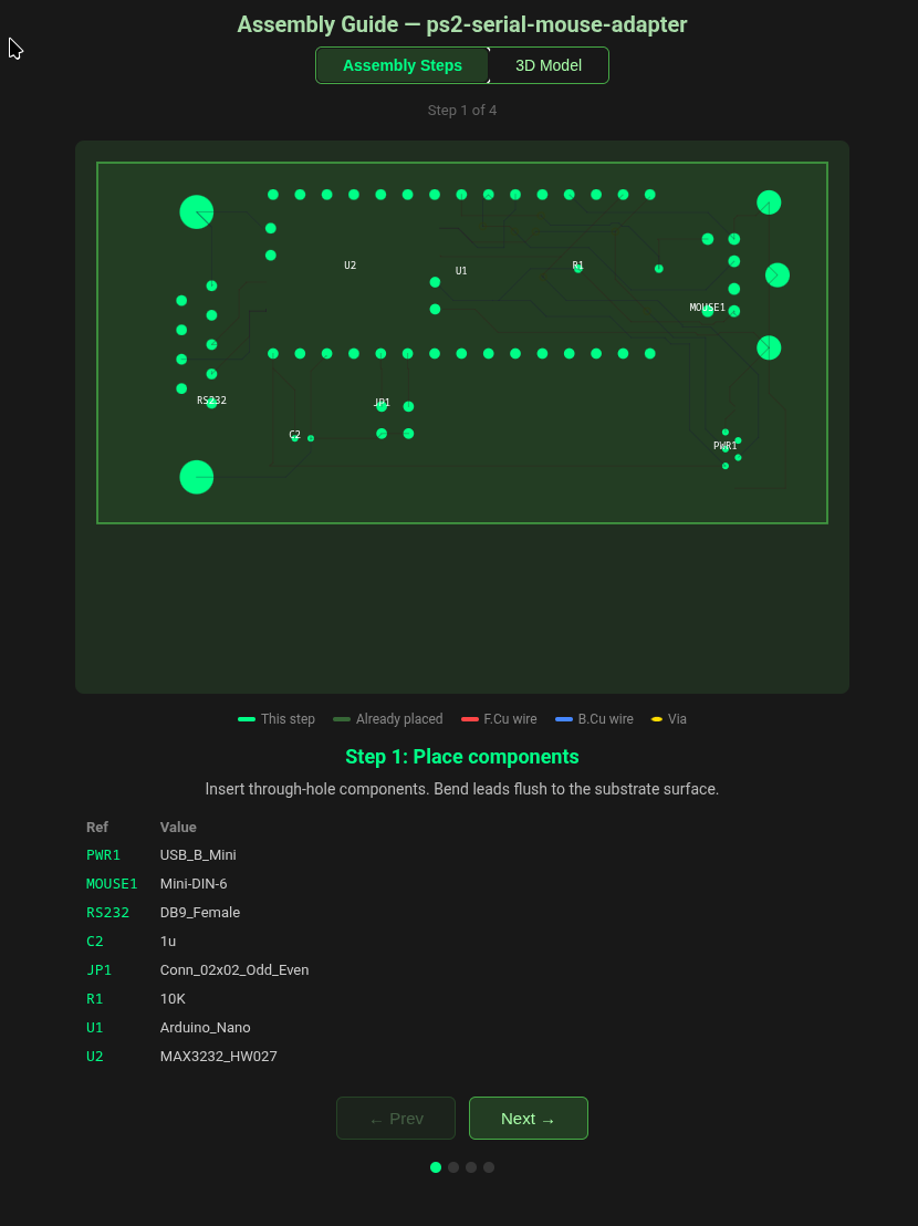
The hybrid PCB method breaks that loop entirely. You 3D print a substrate with grooved channels for traces and holes for component pads. Copper wire lays into the channels as traces; copper eyelets connect the layers. Solder your components as you normally would. The result is a functional board produced at home in a couple of hours — no chemicals, no etching, no MOQ.
kicad2print handles the conversion step: it reads your .kicad_pcb
file and produces a print-ready STL or 3MF substrate model, plus a self-contained interactive
HTML 3D preview so you can inspect the board before slicing. It also ships an MCP server
that lets Claude Desktop read and make targeted edits to KiCad projects — swap a footprint,
check the BOM, run DRC — without leaving the chat window.
A personal project born from wanting to build electronics faster than fab houses allow.
Five steps from KiCad design to working board — no fab house required.
.kicad_pcb files — no plugin or export step needed.
kicad2print my_board.kicad_pcb. The tool parses the PCB, auto-scales if needed so the narrowest trace fills a channel, tessellates the 3D substrate mesh with grooves and pad holes, and writes an STL/3MF to ./output/. A self-contained HTML 3D preview is generated alongside it.
A clean pipeline from S-expression parser to binary mesh writer, plus an MCP server layer on top.
%%{init: {'theme': 'base', 'themeVariables': {'fontSize': '15px', 'fontFamily': 'Inter, ui-sans-serif, sans-serif', 'lineColor': '#a5b4fc', 'primaryTextColor': '#e2e4ea', 'primaryColor': '#1e2330', 'primaryBorderColor': '#6366f1', 'secondaryColor': '#252b3b', 'tertiaryColor': '#181c26', 'background': '#0d0f14', 'clusterBkg': '#181c26', 'clusterBorder': '#374151', 'titleColor': '#e2e4ea'}}}%%
flowchart TD
    A([".kicad_pcb"])

    subgraph parse["Parse"]
        B["parser/sexp.rs\nTokenize S-expressions → SexpNode tree"]
        C["parser/kicad.rs\nWalk tree → PcbData\n(traces, vias, pads, outline, cutouts)"]
        B --> C
    end

    subgraph transform["Transform"]
        D["autoscale.rs\nScale so narrowest trace fills channel"]
        E["geometry/\nTessellate 3D substrate mesh"]
        D --> E
    end

    subgraph export["Export"]
        F["export/stl.rs\nBinary STL"]
        G["export/threemf.rs\n3MF (ZIP + XML)"]
        H["export/html.rs\nSelf-contained three.js preview"]
    end

    subgraph mcp["MCP Server (--mcp flag)"]
        I["14 tools\nscan, render, DRC, BOM,\nfootprint ops, convert…"]
    end

    A --> B
    C --> D
    E --> F
    E --> G
    E --> H
    A -->|kicad-cli| I
channel_width_mm, the entire board is scaled up so the narrowest trace exactly fills one channel. Component spacing scales proportionally. Override with scale_factor > 0 for a fixed scale.
indent (recommended) prints shallow dimples at via locations — no drilling, press eyelets straight in. hole prints full through-holes for precision drilling after the fact. Configurable per project.
kicad2print.toml in your project for persistent per-board settings; override on the fly with flags without touching the file.
kicad2print --mcp starts the MCP server. Same binary, same install. The server exposes 14 tools that wrap kicad-cli and the conversion pipeline — scan a project, render the board, swap a footprint, run DRC, or generate the substrate, all from Claude Desktop.
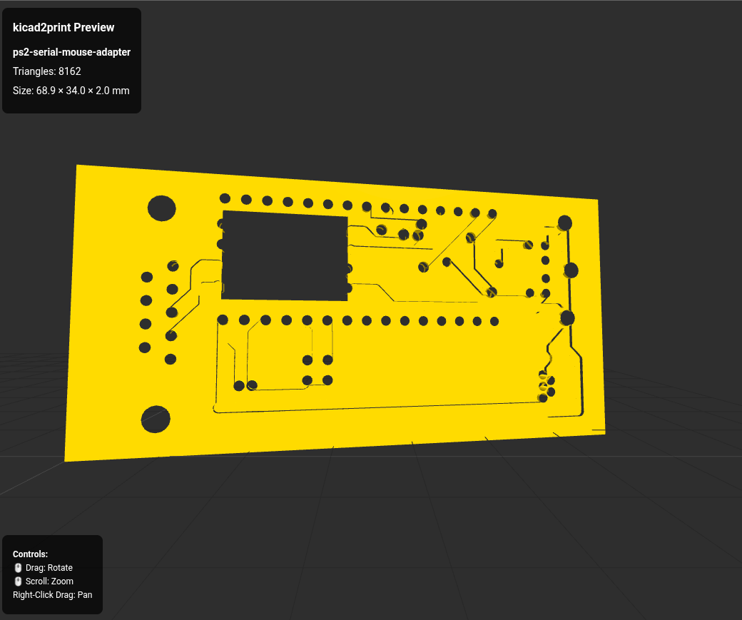
*_preview.html bundles three.js inline — no server, no CDN, no internet required. Open it in any browser and rotate the substrate model before committing to a print.
Running kicad2print --mcp exposes 14 tools to Claude Desktop for reading,
editing, and converting KiCad projects without leaving the chat window.
scan_project
Start here. Renders the board, returns the full BOM and file list in one shot. The recommended first call for any new project.
render_pcb
Render the board from top, bottom, or side views via kicad-cli. Returns the image inline in Claude Desktop.
run_drc
Run the KiCad Design Rules Check. Returns a JSON report of violations — useful for a quick sanity check after footprint edits.
replace_footprint
Swap a component footprint in the PCB file. e.g. change an Arduino Uno to a Nano without opening KiCad. Writes back and re-renders automatically.
convert_pcb
Convert the PCB to a 3D-printable substrate. Runs the full kicad2print conversion pipeline and returns the STL/3MF path + preview link.
export_bom / export_netlist
Export a CSV bill of materials or full component + net connectivity for use in procurement or downstream tooling.
Additional tools: move_component, search_footprint,
list_footprint_libraries, get_footprint,
export_layer_svg, read_kicad_file,
write_kicad_file, get_board_outline.
Download a binary from the Releases page, or build from source with Rust 1.70+.
Install (Linux)
chmod +x kicad2print-linux-x86_64
sudo mv kicad2print-linux-x86_64 /usr/local/bin/kicad2print
Convert a PCB
# Basic conversion — STL/3MF + HTML preview to ./output/
kicad2print my_board.kicad_pcb

# With custom channel width and eyelet style
kicad2print my_board.kicad_pcb --channel-width 0.8 --eyelet-style hole

# Generate both formats and open the preview
kicad2print my_board.kicad_pcb --format both --view
MCP Server — add to Claude Desktop config
{
  "mcpServers": {
    "kicad2print": {
      "command": "/usr/local/bin/kicad2print",
      "args": ["--mcp"]
    }
  }
}
Config: ~/.config/Claude/claude_desktop_config.json (Linux) /
%APPDATA%\Claude\claude_desktop_config.json (Windows).